AMD's Multi-Chiplet GPU for Gaming Is Near; Could Launch with Next-Gen UDNA Architecture
With the new approach, combined with additional shared L3 cache, Team Red hopes to address latency issues; however, this is certainly not a simple task.
The concept of MCM (Multi-Chiplet Module) is not entirely new to the graphics segment, but with the limitations of monolithic designs, the trend towards MCM in the industry is certainly increasing. AMD seems to be one of the most experienced players in multi-chiplet design, with the AI Instinct MI200 series at its core. This is AMD's first generation of GPUs to feature an MCM design with multiple chiplets stacked on a single package, such as GPCs (Graphics Processing Cores), HBM stacks, and I/O dies. With the Instinct MI350 series, AMD has taken a fairly new approach, which if successful will become the foundation for chiplet-based consumer GPUs,
Currently, the biggest limitation of applying chiplet design to gaming GPUs is higher latency, as frames are not tolerant of data having to 'jump' over long distances, and to solve this problem, AMD needs to come up with a solution that bridges the gap between data and computation as closely as possible. Based on a newly revealed patent application, it has been discovered that AMD may have successfully cracked the code for a 'multi-chiplet' gaming GPU. Interestingly, the patent details the CPU instead of the GPU, but the text and mechanism indicate that it is aimed at a graphics use case.
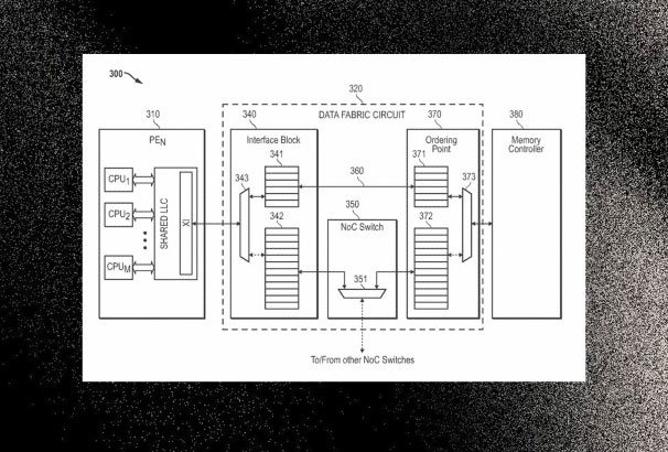
So, how exactly would AMD use a multi-chiplet design with GPUs? The key component in the patent is said to be a 'data-fabric with an intelligent switch' that bridges communication between the compute chiplets and the memory controller. It's essentially AMD's Infinity Fabric, but scaled down for consumer GPUs, since Team Red can't use HBM memory dies. The switch is designed to optimize memory access by first comparing whether a request for a graphics task requires task migration or data replication, with a nanosecond-level latency decision.
Once the data access issue is solved, the patent proposes having GCDs with L1 and L2 caches, similar to what's happening with AI acceleration. However, an additional shared L3 cache (or stacked SRAM) could be accessed via a switch, which would be used to connect all the GCDs. This would reduce the need for global memory accesses, and more importantly, act as a shared staging zone between chiplets, similar to what AMD does with their 3D V-Cache, except it's primarily for the processor. Then there's the stacked DRAM involved, which is essentially the foundation for an MCM design.
What makes this multi-chiplet patent interesting is that AMD is essentially ready for the ecosystem. The company can use TSMC's InFO-RDL bridge and a specific version of Infinity Fabric between the dies for packaging. And what makes this implementation even more interesting is that it's a scaled-down version of the AI accelerator. AMD has previously planned to unify its gaming and AI architectures under a single platform: the UDNA architecture.
Given the limitations of monolithic designs, the graphics industry needs a change, and AMD may have one of its best chances to take the lead. However, there are complications to be addressed with chiplet designs, one of which AMD has already experienced with its RDNA 3 platform, related to latency introduced by the chiplet interconnect. However, with the new approach, combined with additional shared L3 cache, Team Red hopes to address latency issues; however, it is certainly not a simple task.
- Test about computer architecture P6
- Battalion Multi-Touch CZ-10: Multi-touch technology encroaches on laptops
- AMD sets a launch date for the first desktop CPU line based on Zen 5 architecture: Ryzen 9000
- Test of computer architecture P5
- Top cheap gaming CPUs worth buying in 2023
- CES 2020: Intel will launch extremely compact modular gaming PC
- What is Multi TouchPad on laptop?
- MSI launches multi-feature laptops for gamers
- MacBook Air foretells death of hard drive?
- AMD-based netbooks play Full HD videos
- AMD announced the platform for ultra-thin laptops
- Netbooks using AMD Athlon Neo chips weigh less than 1.5 kg
- Scoring CPU for netbook
- MSI X-Slim X430 Laptop: The hidden bar contains power
- The underground war between laptops
- MSI L2100 - AMD Athlon Neo laptop running Windows 7
- AMD felt bad because he was out of the netbook game
- Intel updates the CPU price list for PCs with X 12 series of chips


-
 Comparing AMD and Intel chips, which one should you choose?
-
Update AMD graphics card drivers on Windows 10
-
The price for the AMD Ryzen 9850X3D – the world's fastest gaming CPU on Windows 11 – has been revealed.
-
Battlefield 6 PC Configuration
-
What is AMD CPU? Advantages and disadvantages of AMD CPU
-
Adobe CEO received $12.2 million in salary and bonus in 2010
 Comparing AMD and Intel chips, which one should you choose?
 Update AMD graphics card drivers on Windows 10
 The price for the AMD Ryzen 9850X3D – the world's fastest gaming CPU on Windows 11 – has been revealed.
 Battlefield 6 PC Configuration
 What is AMD CPU? Advantages and disadvantages of AMD CPU
 Adobe CEO received $12.2 million in salary and bonus in 2010