This new type of 3D chip could break through the 'memory wall' that is holding AI back.
The new monolithic 3D chip helps AI overcome memory limitations, promising performance up to hundreds of times higher than traditional 2D chips.
Table of Contents
Engineers from Stanford University, Carnegie Mellon University, the University of Pennsylvania, and the Massachusetts Institute of Technology (MIT) have collaborated with SkyWater Technology—the largest independent semiconductor foundry in the U.S.—to create a completely new type of multilayer computer chip. This design opens up groundbreaking prospects for artificial intelligence hardware and strengthens efforts to bring advanced semiconductor manufacturing back to the U.S.
Unlike traditional 2D chips, where components are laid flat on a single surface, the new chip prototype stacks multiple layers of ultra-thin circuitry vertically. Vertical connections link these layers, allowing data to move much faster between memory and processing units.
The densely oriented vertical wiring network, combined with tight integration of memory and computing power, overcomes the long-standing limitations of planar chip design. Test and simulation results show that this 3D chip delivers approximately an order of magnitude higher performance than traditional 2D chips.
While there have been many previous experimental studies demonstrating 3D-cut chips, this is the first time such a design has shown both clear performance benefits and been manufactured in a commercial foundry. ' This opens the door to a new era of chip manufacturing and innovation, ' said Professor Subhasish Mitra (Stanford), lead researcher, at the 71st IEEE IEDM Conference. ' Breakthroughs like this are the path to achieving the 1,000-fold hardware improvements that future AI systems will require. '
The problem with flat chips
Modern AI systems like ChatGPT or Claude rely on the ability to move massive amounts of data between memory – where information is stored – and computing units – where the data is processed.
On a standard 2D chip, these components are on the same plane with a very limited amount of contiguous memory. Therefore, data is forced to travel along a few long and congested 'highways'. While the processing units operate extremely fast, data transfer speeds lag behind, and the lack of local memory causes constant system delays. Engineers call this limitation the 'memory wall,' where processing power far exceeds the chip's data-providing capacity.
For decades, the semiconductor industry has tried to solve the problem by shrinking transistors and cramming more and more components onto a single chip. However, this strategy is also approaching a physical limit, known as the 'miniaturization wall'.
The new chip overcomes both of these barriers by… building vertically. ' By integrating memory and computing vertically, we can move large amounts of data much faster, much like elevator systems in high-rise buildings that allow many people to move between floors at the same time ,' explains Tathagata Srimani (Carnegie Mellon), the lead author of the study.
Robert M. Radway (University of Pennsylvania) stated: " The memory wall combined with the shrinking wall creates a deadly combination. We confront this head-on by integrating memory and logic extremely tightly, then building on top of it with very high density. It's like the Manhattan of computing – cramming more 'people' into a smaller space ."
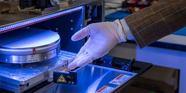
How are the new 3D chips manufactured?
Previously, most efforts to make 3D chips relied on stacking individual chips. This method worked, but the connections between the layers were often rough, loose, and prone to becoming bottlenecks.
Instead of fabricating each chip separately and then assembling them, the research team built each circuit layer directly on top of the previous one in a continuous process. This 'monolithic 3D' method uses temperatures low enough not to damage the layers underneath, allowing for denser component stacking and much higher connectivity.
Most notably, the entire process was carried out in a commercial foundry in the United States. ' Transforming a pioneering academic idea into something commercially viable is an enormous challenge ,' said Mark Nelson, Vice President of SkyWater Technology. ' This research demonstrates that advanced architectures don't just exist in the lab, but can be manufactured domestically on a large scale – something the U.S. needs to maintain its semiconductor leadership .'
Performance and potential
Initial hardware tests showed the prototype chip was about four times faster than a comparable 2D chip. Simulations of a higher-end future version – with more memory and computing layers – showed even greater improvements. Some multi-layer designs achieved up to 12 times the performance in real-world AI tasks, including workloads based on Meta's open-source LLaMA model.
Most notably, the research team believes this design opens a practical path to achieving 100 to 1,000-fold improvements in Energy-Delay Product (EDP) – a measure of the balance between speed and energy efficiency. By minimizing the data travel distance and adding numerous vertical 'lanes,' the chip can process data faster while consuming less power – something that previous flat chip architectures were nearly impossible to achieve.
According to the scientists, the long-term significance of this research lies not only in performance. Demonstrating that monolithic 3D chips can be manufactured right here in the United States has laid the foundation for a new era of domestic hardware innovation, where the U.S. can both design and manufacture the most advanced chips.
Just as the integrated circuit revolution of the 1980s was driven by students learning to design and fabricate chips in American labs, the shift toward vertical 3D integration will also require a new generation of engineers proficient in these technologies. Through collaborative programs and grants like the Northwest-AI-Hub, students and researchers have been and are being trained to advance American semiconductor innovation.
' Breakthroughs like these are obviously about performance ,' concluded Professor H.-S. Philip Wong (Stanford), ' but more importantly, they're about capability. When we can build advanced 3D chips ourselves, we'll innovate faster, react more quickly, and proactively shape the future of AI hardware. '
Was this article helpful?
Your feedback helps us improve.
Related Articles
 Samsung's new memory chip incorporates EUFS 3.0 technology, recording speed of 2100MB / s, copying Full HD movies in just 3 seconds2 minutes read
 Why should you install an additional USB wall outlet?5 minutes read
 Package-on-Package technology: Reduce cellphone size2 minutes read
 Samsung began mass-producing the world's 'fastest memory' for smartphones2 minutes read
 Data type in C / C ++3 minutes read
 China's memory chip production will go from zero to 5% of the world by the end of next year5 minutes read
Reader Comments 0
Sign in with email or Google to join the discussion.