How is the CPU produced?
We use computers every day and an indispensable part is the CPU, but have you ever wondered how the CPU was created? This article will introduce you to the Intel process of making a CPU for your computer.
We use computers every day and an indispensable part is the CPU, but have you ever wondered how the CPU was created? This article will introduce you to the Intel process of making a CPU for your computer.
CPU derived from sand
Sand is made of 25% silicon, just behind oxygen, it is the second richest chemical element in the earth's crust. Sand, especially quartz, has a high proportion of silicon in the form of silicon dioxide (SiO2) and is a basic component for semiconductor manufacturing industry.

Refined and developed
After purchasing coarse sand and silica separation, excess material will be processed and silicon is refined in several steps to finally achieve the quality of semiconductor manufacturing, known as electronic silicon. The purity after refining is so great that silicon at the electronic level has only one strange atom for every billion silicon atoms. After the refining process, Intel performs silicon melting. The result is a single crystal block (mono-crystal).

Single crystal block
Single crystal blocks are produced from silicon at the electronic level. This block weighs about 100 kg (or 220 pounds) and has a purity of 99.9999%.

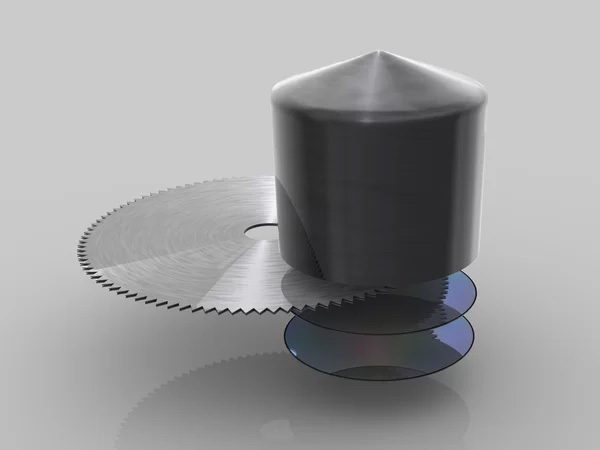
Cut a single crystal block
Then, the single crystal block will be cut thinly into semiconductor discs or called wafer plates. Some blocks will be cut with a thickness of over 5 feet because the block diameter size varies depending on the size of the wafer required. Today, CPUs are usually made of wafers with a diameter of 300mm.
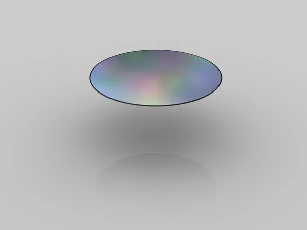
Polishing wafers
After the cutting phase, these wafers will be polished until they have a smooth, smooth surface. Intel does not produce crystals and wafers, they will buy from other companies. Intel's 45 nm High-K / Metal Gate process uses wafers with a diameter of 300mm (or 12 inches). When Intel first produced chips, they printed circuits on 50 mm (2 inch) panels. Today, Intel uses a 300 mm semiconductor plate, which reduces production costs for each chip.
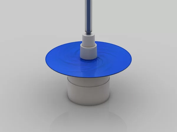
Using contrast material (Photoresist)
Blue liquid as shown below is a contrast material like the one used in film cameras. In this step, the wafers will be rotated so that the contrast material can be evenly covered, smooth and thin on it.
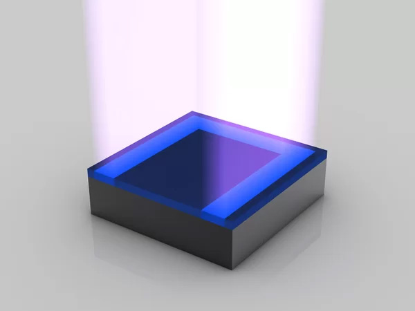
Exposure with ultraviolet rays
At this stage, the anti-reflective finish will be exposed with ultraviolet (UV) light. The chemical reaction activated by ultraviolet light is similar to what happens to film materials in a camera as soon as you press the shutter button.
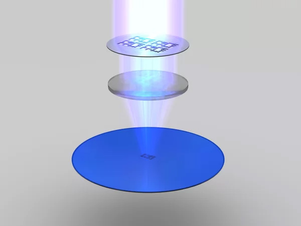
The areas of contrast material on the wafer that have been exposed to UV light will become soluble. Intel will use masks as templates with ultraviolet light to create different circuit patterns on the wafer. Creating a major CPU repeats this process continuously until multiple layers are stacked.
A lens (middle) reduces the image of the mask to a small focus. The "print" result on the wafer is usually 4 times smaller than the pattern of the mask.
Make more exposure
The image below shows what a transistor looks like when viewed with the naked eye. Transistors are considered electronic switches, controlling the current in a computer chip. Intel researchers have developed transistors that are so small that they think 30 million transistors can fit in one end of the battery.
Wash the contrast material
After exposure to ultraviolet rays, areas with exposed blue contrast material will be thoroughly cleaned with solvent. This will reveal the contrast pattern made by the mask.
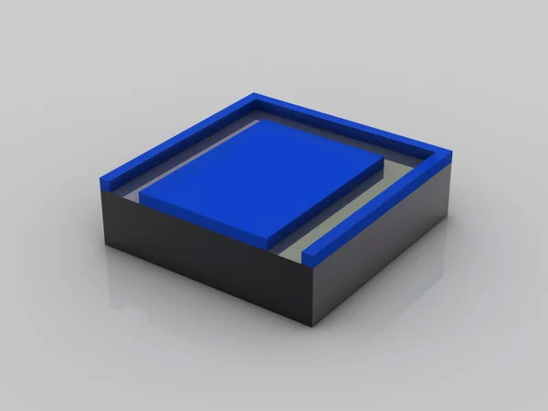
Notch
The reflective layer will protect the semiconductor material from being cleaned. The exposed areas will be etched with chemicals.
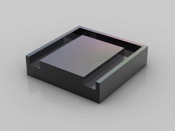
Removal of contrast material
After carving, contrast material will be removed and you can see the desired shape.
Use more contrast materials
At this stage, Intel uses more contrast material (blue) and then exposes it to ultraviolet rays. After that the dye is exposed to be washed before moving on to the next step. This is the step where ionic particles are exposed to water, altering the chemical properties of silicon so that the CPU controls the current.
Ion Doping (Ion etching)
Through a process called ion implantation (a form of doping process) the wafer exposures are etched with ions. The ions that are implanted in the wafer will change the way silicon in these areas conducts electricity. Ion is pushed to the surface of the wafer at very high speeds, an electric field accelerates ions at a rate of over 300,000 km / h (about 185,000 mph).
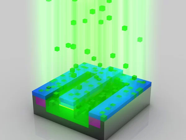
Wash the contrast material
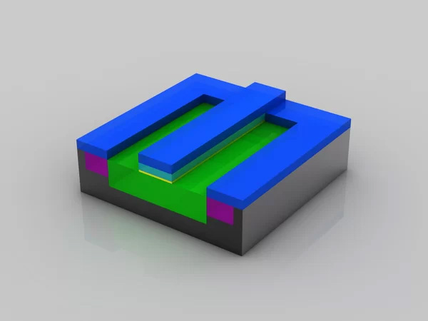
After ion implantation, the dye will be removed and the material to be etched (green) now has strange atoms implanted.
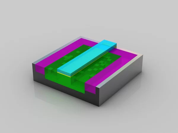
Transistors
Transistors are almost about to be completed. Three holes were etched into the insulation (dark pink) above the transistor. These three holes will be filled with copper, forming connections with other transistors.
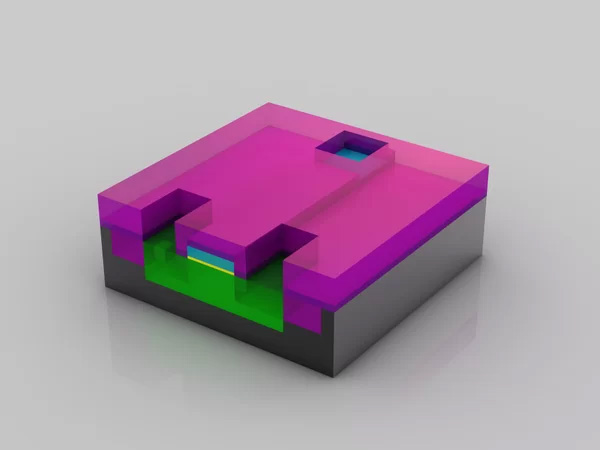
Wafer electroplating technique
The wafers are fed into copper sulfate solution at this stage. Copper ions are deposited into transistors through a process called electroplating. Copper ions travel from the anode (anode) to the cathode (cathode).
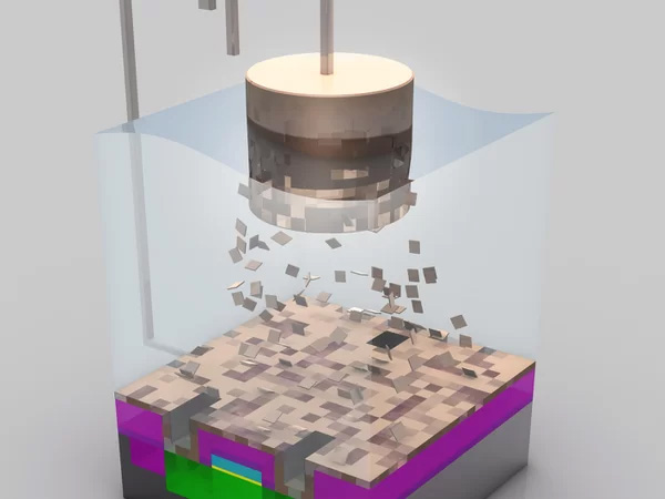
Arrange ion
Copper ions will be arranged into a thin layer on the wafer surface.
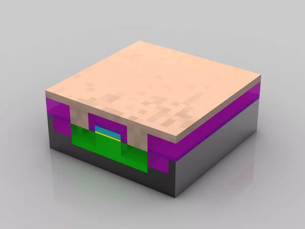
Polish excess
Polished excess materials leave a thin layer of copper.
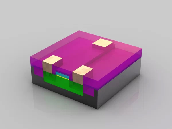
Create class
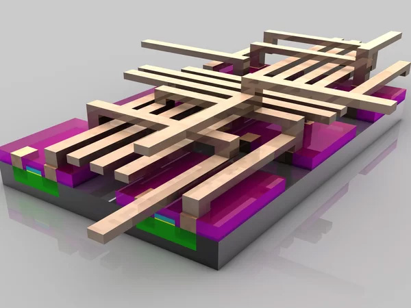
Many metal layers are created to connect between different transistors. Intel's architecture design and construction team determines how these connections are interconnected according to their respective processor functions (for example, Intel's Core i7 processor). Although computer chips look extremely flat, they can hold up to more than 20 layers to form complex circuits. If a room is large, you will see a complex network of wires and transistors that look like a multi-level highway system.
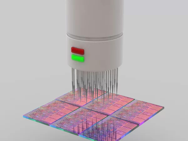
Check the wafer
A small part of the finished wafer will be put into the first functional test. During this phase, the test sample will be included in each single chip and monitored, comparing the response from each chip.
Cutting wafer into die
After the test determines that the wafer has good performance in processing devices, it will be cut into pieces called die.
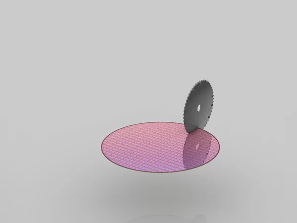
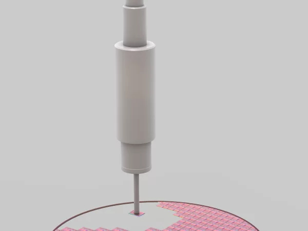
Check the die
The dies that respond properly to the control patterns will be moved to the next step (packaging), the bad dies will be removed.
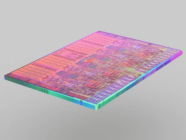
Die
This is a separate die that has been cut from the previous step (wafer cutting). Die in this image belongs to an Intel Core i7 processor.
Packed CPU
The substrates, dies and heat exchangers are combined to form a complete processor. The green substrate creates the electrical and mechanical interface for the processor to interact with the rest of the computer system. Silver heat exchanger is a thermal interface, used for cooling solutions. This will make the processor cool during operation.
- 5 ways to cool down, cool, laptop radiator simple and effective

A complete CPU
Processors are the most complex manufactured products. In fact, it takes hundreds of steps and here comes only the most important steps.
CPU test
In this final test, the microprocessor will be tested for key characteristics (among the properties tested are the maximum power dissipation and frequency).
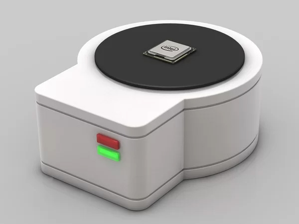
Classify CPU
Based on the classification test results, processors with the same capacity will be included in the same shipping tray. This process, called binning, must be familiar to Tom's hardware readers. Binning determines the maximum operating capacity of a processor, divided by batch and sold according to stable specifications.
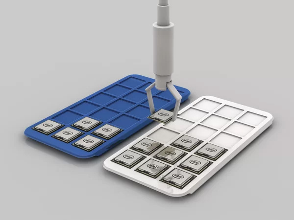
CPU distribution
Processors are manufactured and tested or go to system manufacturers or to retail stores.
You can watch this video to get a better understanding of the CPU production process.
See more:
- Learn about how the CPU works
- How to choose laptop CPU that meets the needs (part 1)
- Which CPU is faster: old but 'quality' or 'popular' but new?
- In the future, protein-rich foods will be produced from electricity and CO2
- Bphone has 2 huge configurations, 5.5 inch screen, 4GB RAM, 21MP camera
- 50% of Samsung phones are manufactured in Vietnam
- There will be Sony Vaio computers produced by third parties
- Netbook costs 1.8 million
- Collection of some sleek netbooks


 Why is the CPU or rectangular camera sensor created from a circular plate?
  How computer chips are produced