Table of Contents
This guide provides a practical overview of Shortcuts in Altium Most Often Used, including its main features, benefits, limitations, and important considerations.
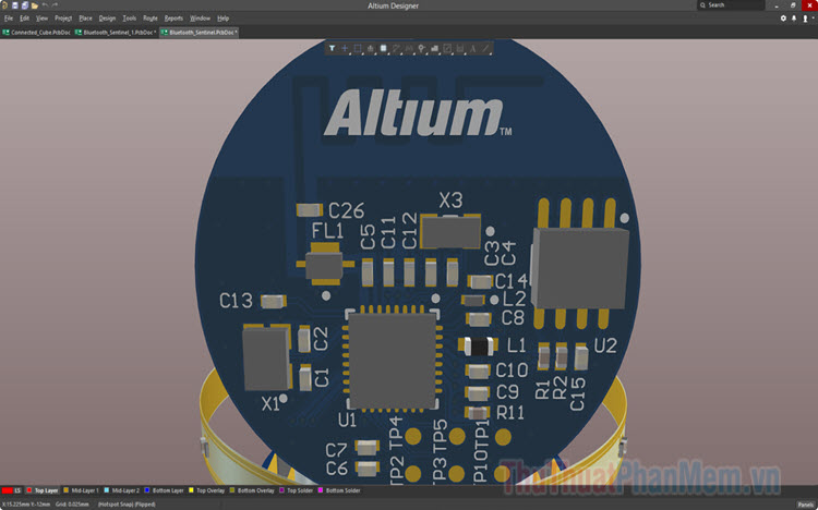
1. Shortcuts in circuit design principle (Schematic)
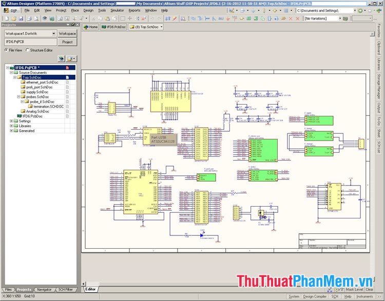
Function
X
Rotate components in the horizontal axis (X axis).
Y
Turn the device on the vertical axis (Y axis).
Space
Rotate components 90 degrees
Shift + Space
Rotate components 45 degrees.
Ctrl + Click and drag
Move the device that comes with the cord (Like in Proteus)
Shift + Left Click
Copy components.
Shift + Click and drag
Pull the device out.
Ctrl + Shift + L (or AL)
Align the components vertically.
SPACE
Change color when using Highlight pen (Highlight the NET of the same name)
ALT + Click (select Net)
Highlight the NETs with the same name (Blur all the rest of the SCH drawing)
Shift + Ctrl + C
Delete the settings on SCH
Ctrl + Shift + T (or AT)
Align the components horizontally.
Ctrl + Shift + H (or AH)
Align the components evenly spaced horizontally.
Ctrl + Shift + V (or AV)
Align components evenly in vertical rows.
Ctrl + M
Measure the distance.
C, C
Compile Project - Check connection errors, port.
D, B
Get components in the library.
D, O
Change drawing parameters.
D, U
Transfer principle to printed circuit board.
J, C
Jump to the components.
P, B
Draw bus routes.
P, N
Name the line.
P, O
Get the GND
PT
Add Text.
P, W
To connect the component pins.
P, V, N
Use vacuum marking.
T, A
Open the naming management window for components.
T, N
Automatic naming of components.
T, S
Find components on the printed circuit board (You select the block you need to wire the circuit and then press TS, it will automatically find the printed circuit block for you).
T, W
Create new components
TAB
Change the parameters of the circuit.
V, D
Align the drawing to fit the screen frame
2. Shortcuts in PCB printed circuit design
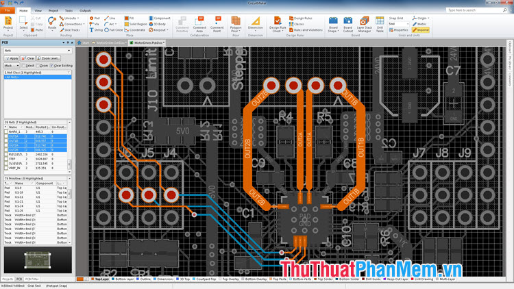
Function
2
See printed circuit in 2D format.
3
See printed circuit in 3D.
Q
Convert miles => mm and from mm => miles
PT
Switch to manual wiring.
P, L
Resize the printed circuit size, click the keep out layer to draw the outline, then highlight the whole circuit and press DS D.
PM (Altium 16) UM (Altium 17)
Drag multiple wires at once (MultiRoute) (by: pressing Shift to select multiple Pad, then press [PM] / [UM] and then go to the wire as usual. While MultiRoute, you can press Tab to adjust the distance relative to each other)
P, G
Coated with copper.
P, V
Take a Via hole.
P, R
Draw large circuits, the distance between small circuits.
P, D, D
Show PCB size information
A, A
Automatic wiring.
T, U, A
Erase all running circuits.
T, U, N
Delete lines of the same name.
T, D, R
Check whether the wiring is complete after completing manual wiring.
T, E
Round the line near the component pins
T, M
Clear the error displayed on the screen.
D, K
Select the drawing layer. (Stack Manager)
D, R
To adjust parameters in the circuit such as the width of the line (Width), the distance 2 - wire (Clearance), allows short circuit (Short circuit).
D, O
Adjust the circuit parameters, if you do not want the squares to affect the circuit, then convert the line into dots.
D, T, A
Show all layers.
D, T, S
Show only TOP + BOTTOM + MULTI layers.
C, K
Open the component path editing window.
R, B
Display circuit information (size, number of components.)
O, D (Or Ctrl + D)
Display the Configurations window (Adjust the visibility of components)
V, B
Rotate the drawing 180 degrees.
V, F
Show the whole drawing.
L
When moving components flip over components Top and Bottom (Bottom and Top)
Ctrl + Shift + L (or AL)
Align the components vertically.
Ctrl + Shift + T (or AT)
Align the components horizontally.
Ctrl + Shift + H (or AH)
Align the components evenly spaced horizontally.
Ctrl + Shift + V (or AV)
Align components evenly in vertical rows.
Ctrl + Shift + Mouse scroll
Switch between classes.
L or Ctrl + L
Open View Configuration to adjust the display of layers.
TAB
Show information window changes during operation.
Fliped Board
Turn over the printed circuit.
Ctrl + G or G
Grid mode settings.
Ctrl M
Measure the size of the circuit.
Shift + M
Square magnifying glass.
Shift + R
Change the wiring mode (Cut - No cut - Push rope).
Shift + S
Only allow one layer currently selected (the remaining layers are hidden).
Shift + Space
Change the line mode (Free - By law - 90 degree Square - Curved)
3. Shortcut key in 3D visualization mode

Function
0
Turn the board back to default
9
Rotate the board at a 90 degree angle
2
Switch to 2D mode when in 3D View mode
3
Switch to 3D View when in 2D mode
SHIFT
Simultaneously press Shift and Right click, move mouse to rotate the circuit board in XYZ axes
SHIFT + Mouse scroll
Left - Right
CTRL + Mouse scroll
Zoom in - Zoom out
CTRL + Move the mouse
Zoom in - Zoom out
V, F
Align the board to fit the screen
V, B
Flip the circuit boad
Scroll the mouse
Pull up - Pull down
CTRL + C
Take a photo of the current view of the 3D board on the Clipboard, to save as an image file you need to use a tool like Paint.
T, P
Open the Preferences window
L
Open the Configurations window
Memorizing and mastering shortcuts on Altium is quite difficult and we can only achieve by practicing and using shortcuts frequently. Good luck!
FAQ
What should I know about Shortcuts in Altium Most Often Used?
Focus on the key features, requirements, limitations, and practical use cases explained in this guide.
How do I get the best results with Shortcuts in Altium Most Often Used?
Follow the recommended steps, use current software or information, confirm compatibility, and review settings before major changes.
Are there any risks or limitations?
Potential limitations depend on compatibility, data quality, cost, privacy, support, and how the product or method is used.
Related Articles
 All the Keyboard Shortcuts on Obscure Computers11 minutes read
 Are You Using the Full Potential of the Shortcuts App on Your iPhone?8 minutes read
 Android App Shortcuts That Many People Overlook: Explained4 minutes read
 How to Fix the Problem of Not Seeing Shortcuts on iPhone, iPad7 minutes read
 All Ipad Shortcuts to Build Siri Shortcuts13 minutes read
 28 Windows 11 Shortcuts You Should Know and Use Often5 minutes read
Reader Comments 0
Sign in with email or Google to join the discussion.