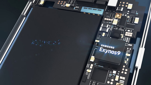
Samsung announced a 3nm process chip, saving more than 50% energy, 35% faster than 7nm chip
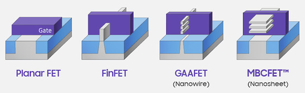
This new 3nm chip is based on the Gate All Around architecture, which helps bring chips smaller than 45% in size.
Samsung recently announced 3nm chip manufacturing technology, at the Samsung Foundry Forum event on Tuesday. This is a new breakthrough in processor technology, which saves energy by more than 50% while increasing performance by 35% compared to Samsung's existing 7nm chips.
This new 3nm chip is based on the "Gate All Around" architecture, which helps bring chips smaller than 45% in size.
In 2020, Samsung will begin to test the 3nm chip and will mass produce for smartphones and mobile devices by 2021.
A more refined version for high-performance chips must wait until 2022 to be mass-produced.
With GAA technology, the channel will be completely surrounded by the gate instead of blocking the polarity as the current FinFET technology. In Samsung's design, the channels in GAA architecture are flat channels, called nanosheet, while some other manufacturers envision them as extremely small cylinders called nanowires. (nanowires).
Samsung expects this new 3nm chip manufacturing technology, with its energy saving advantages, will help it attract more customers.
Handel Jones, head of International Business Strategies, said that with GAA technology, Samsung is about 12 months ahead of TSMC and 2 to 3 years ahead of Intel.
Was this article helpful?
Your feedback helps us improve.
Related Articles
 Samsung announced the new LPDDR5X memory chip with extremely fast speed and excellent energy saving capabilities3 minutes read
 Samsung announced 2nm SF2Z chip manufacturing technology, a new solution for high-quality AI products4 minutes read
 Meaning of energy ranking labels saves electricity on appliances3 minutes read
 Samsung's new memory chip incorporates EUFS 3.0 technology, recording speed of 2100MB / s, copying Full HD movies in just 3 seconds2 minutes read
 Samsung has completed the basic design of the 2nd generation 2nm GAA process, expected to be applied to future Exynos chips.3 minutes read
 Samsung began manufacturing 20nm DRAM 6Gb chips for mobile devices1 minutes read
Reader Comments 0
Sign in with email or Google to join the discussion.