Table of Contents
This updated overview organizes the essential information about Samsung Announced 2nm SF2Z Chip Manufacturing Technology, a New, including practical uses, key features, setup considerations, and common questions.
Along with TSMC and Intel, Samsung is the third company in the world capable of producing advanced semiconductors with the latest fabrication technology. On the event stage, the Korean company introduced advanced variants of the 2-nanometer and 4-nanometer process, while also emphasizing the importance of ultra-high quality transistor designs called Gate All Around (GAA) on the future of the semiconductor chip industry.
The focus of the Samsung Foundry Forum is the introduction of two of the company's new semiconductor manufacturing processes: Samsung SF2Z and Samsung SF4U. In particular, SF2Z is the company's most advanced molding process to date, and is the third version of the 2 nanometer process known as Samsung SF2. With SF2Z, Samsung has caught up with other chip manufacturers in the market such as Intel and TSMC in its ability to optimize the power delivery efficiency of its processors.
Similar to the way other manufacturers do, Samsung will allow its chips to receive energy through the 'back side' of the semiconductor wafer. This area has lower resistance and, according to the company, the back-end power distribution network (BSPDN) will help improve the power, performance and area (PPA) of the chip, while ensuring that the processor is always powered stable voltage - a very important requirement for high-performance computing applications.
Applying BSPDN technology to SF2Z is confirmed by Samsung to help increase power, performance and area (PPA) compared to SF2 - the first generation 2nm node, while significantly reducing voltage drop, improving the performance of HPC designs (high performance computing architecture).
BSPDN is not a new concept in the industry and some of the first rumors about this technology appeared last April. Some sources say TSMC will use BSPDN for an advanced variant of the 2-nanometer process called N2P. However, TSMC confirmed earlier this year that while N2P will not have BSPDN, its next-generation chip manufacturing process called A16 will.
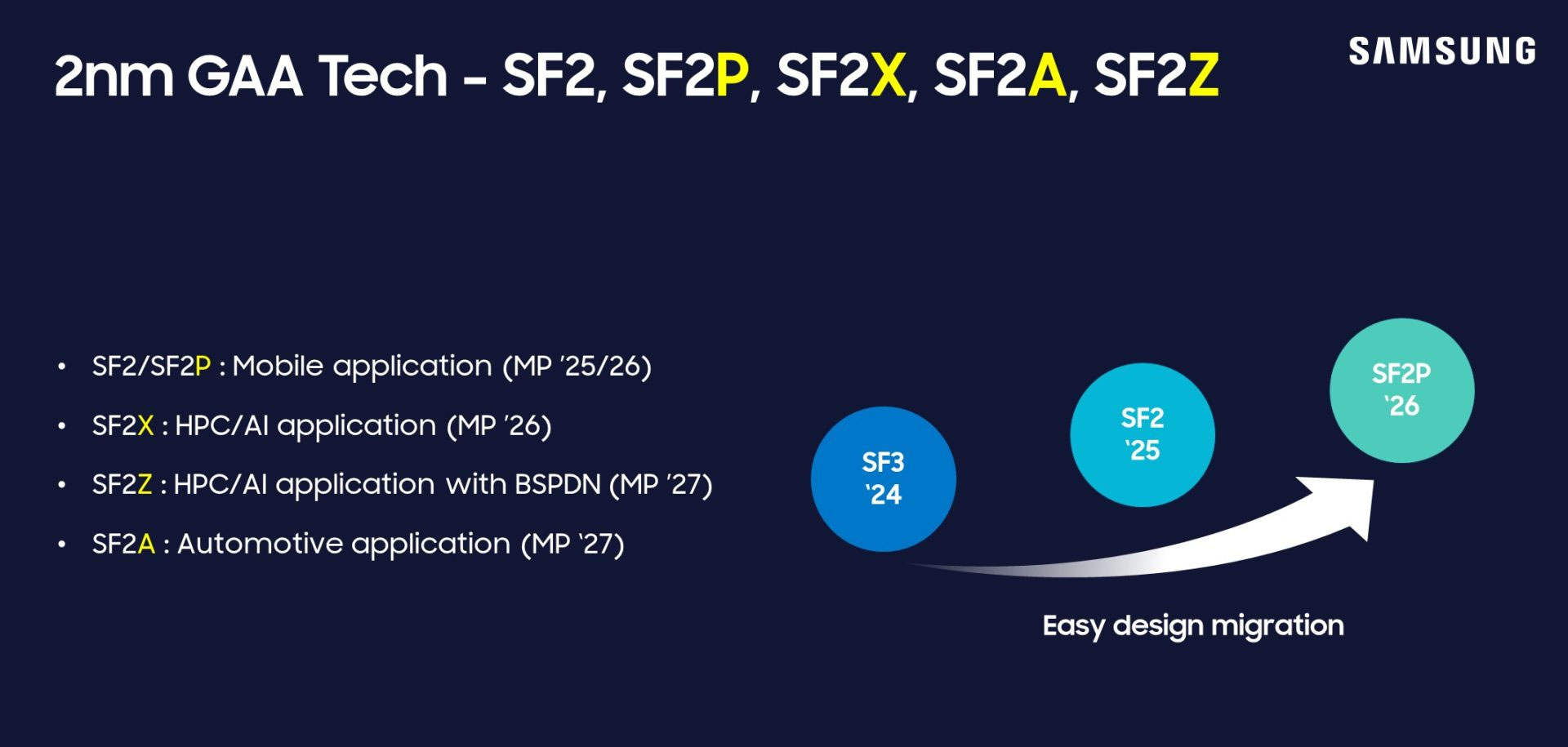
Samsung's second new process technology is the SF4U, which incorporates a scaled-down variation of previous designs. The SF4U can be considered a PPA-enhanced 4nm process node using optical miniaturization technology, allowing the miniaturization of existing chip die designs without much architectural change.
Samsung also shared details about its next-generation chip manufacturing process called SF1.4. The SF1.4 is scheduled for mass production in 2027, and is also set to meet productivity and performance targets. The company added that it will begin mass production of its second-generation 3nm process technology in the second half of this year.
To address the expected impact of AI on the semiconductor industry, Samsung also announced an off-the-shelf chip manufacturing service called Samsung AI Solutions. The Korean manufacturer shared that Samsung AI Solutions will combine the company's foundry, memory and packaging departments to provide a 'turnkey' platform that allows customers to reduce development and design time custom chips.
Final Thoughts
Use the instructions and checks above in order, verify the result after each major step, and keep a backup whenever the process changes important files or system settings.
FAQ
What is Samsung, chip, semiconductor used for?
Along with TSMC and Intel, Samsung is the third company in the world capable of producing advanced semiconductors with the latest fabrication technology.
Who should consider Samsung, chip, semiconductor?
It is most useful for readers who need the features, workflow, or problem-solving approach described in this guide.
What should I check before using it?
Review compatibility, current software requirements, privacy or security settings, costs, and any limitations that could affect your workflow.
Related Articles
 Samsung Began Manufacturing 20nm DRAM 6gb Chips for Mobile Devices3 minutes read
 Samsung Announced a 3nm Process Chip, Saving More Than 50% Energy, 35% Faster Than 7nm Chip3 minutes read
 Samsung's New Memory Chip Incorporates EUFS 3.0 Technology, Recording Speed of 2100MB/s, Copying3 minutes read
 Samsung Started Manufacturing Aquabolt: 2.4G Gb DRM Speed 8GB 2.4Mb/sec3 minutes read
 China Launches Xizhi Lithography Machine: 0.6nm Precision Approaches3 minutes read
 Chip Manufacturing: Complete Guide4 minutes read
Reader Comments 0
Sign in with email or Google to join the discussion.