How computer chips are produced
Have you ever known how chips such as processors, video processors, memory, chipsets, etc. are produced? In this tutorial, we will introduce the necessary information so that you can understand the basics of the process.
Have you ever known how chips such as processors, video processors, memory, chipsets, etc. are produced? In this tutorial, we will introduce the information you need to understand the basics of the chip manufacturing process.
Semiconductor manufacturing process can be summarized through the following steps:
-
Chip design: This is the step that architects design chips, which means how it will work.
-
Wafer fabrication: This is the main process in chip manufacturing and we will look into it in this tutorial.
-
Prepare stereotypes: This step basically involves cutting chips from wafer
-
Package: In this step, the terminal and the main part are added to the chip
-
Test: The chip is tested before being sold.
Each step in the above steps is further divided.
When it comes to 'chip production' it is often that we think about the manufacturing step, this is the most complicated step. And this is the step that we will explain in this tutorial.
The process of manufacturing raw wafer
Wafer is a base on which chips will be built. Raw wafers are made of silicon, a compound of sea sand. They are made through a process called Czochralski, where a piece of silicon crystal has a rod-shaped structure that is then embedded in molten silicon. This rod structure will be pulled and rotated simultaneously, creating a large cylindrical piece of silicon crystal, this large piece of crystal is still known as ingot.
The ingot produced in this process is about 1 to 2 meters long and can have a diameter of up to 300mm (this is the origin of the 300-mm wafer term we still use today).

Figure 1: The ingot is cut thin to create coarse wafer
A common question here is why the wafer has a circle and not a square. The answer to this is simple. The reason is that through the Czochralski process, this ingot is created by pulling and rotating while the silicon melts, so the natural shape of the silicon crystal created in this process will be round but not is square.
Printing technique
Chips are on the wafer through a process called printing technique. Under this process, chemical substances are strongly affected by radiation light. When exposed to these radiation rays, they can become soft or hard. So basically this process involves blocking radiation beams for the chemicals applied to the wafer by using substrates (or masks created by engineers), removing the into software and then repeat this process again with another mask, this process is repeated until the chip is done.
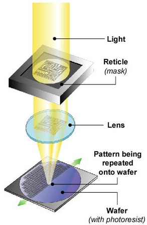
Figure 2: How printing is done
Obviously each mask has different patterns and they are the way transistors and wires inside the chip are built. The number of masks used also varies depending on the given project. For example, Pentium 4 processors use up to 26 masks.
Let's look at exactly how this process is done.
The first thing that is done to the raw wafer is to implant silicon dioxide (SiO2) on it, by doing this by exposing the wafer to extremely hot temperatures and gas. This implant is similar to the way that iron adheres to a metal surface when exposed to a wafer, but it will happen faster.
Next the wafer is made of a material called photoresist, which is a substance that can be dissolved when exposed to radiation. The first mask is applied and the wafer is exposed to radiation. The software of photoresist is separated by a solution and then the components of the exposed silicon dioxide layer are separated during the acid separation process. The excess of the photoresist is removed, so now we have a wafer with a silicon dioxide layer shaped like the first mask.
Another silicon dioxide layer continues to be made on the wafer, large polysilicon is applied on its top surface and then another photoresist layer is applied on them. The second mask is made and the wafer is exposed to a second radiation. The soft photoresist part is removed with a solution and then the polysilicon parts and the silicon dioxide layer are exposed and separated by acid. The excess of the photoresist is removed and now we have a wafer with a silicon dioxide layer with a mold like the first mask and its upper part is a polysilicon and silicon dioxide layers have a pattern of the second mask.
After these two steps, a process called doping (or ionization) will take place. Here the exposed areas of the wafer are bolded with different symbols, aiming to change the pathways of exposed areas to electricity. Exposed areas will be converted into P-type semiconductors (anodes) or S-type semiconductors (cathodes), depending on the chemicals used: Phosphorus, Atimom and arsenic are substances Typically still used to create N semiconductor layers, and Bo, Indium and Gallium are used to create P semiconductor layers. The arrangement of these semiconductor layers creates PNP or NPN transistors.
Creating layers and using masks is repeated many times after the layout of the next mask. A metal will then be pressed into the wafer, filling the holes that have been formed to create a connection between the layers. The process of using masks and acid separation will be done to add electrical connections.
This process is repeated many times until the chip is done, meaning the masks are used up. The production process and the number of layers depend on the components produced. For example, with Pentium 4 processors, they used 26 masks and 7 metal layers.
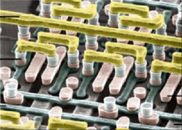
Figure 3: Transistors built inside the chip and connect the metal between them.
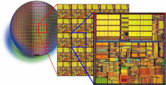
Figure 4: Wafer in Pentium 4 processor after being manufactured
The chips on the wafer after being tested and wafer are sent to the next step in the production process, in this step the chips will be wafer cut, with their end components attached and packaged. They will then be tested, branded and sold.
All the process described above happens inside a room called 'clean room'. You may have seen some pictures of people working in this room with special clothes called 'bunny suits'.
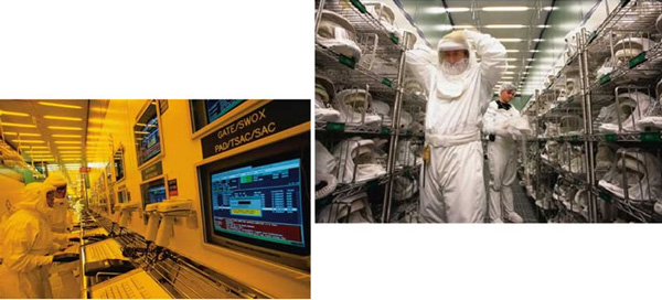
Figure 5: Rabbit costume in clean room
Because we are producing micro-transistors so just a small dirty action can damage the chip, you can see the examples in Figure 6.
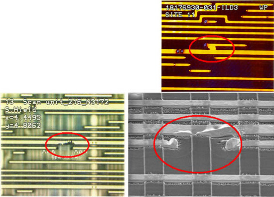
Figure 6: A bit of dirty cleaning can also damage the chip
- Future Macs won't use Intel chips?
- Warning of the risk of businesses being attacked through micro-chips attached to servers
- How is the CPU produced?
- Intel shook hands with Rockchip to produce chips
- For the first time, scientists have successfully implemented quantum shifts between two chips
- Samsung users have been fed up with the Exynos chip
- Apple considers removing Qualcomm chips on iPhones and iPads next year
- Compare the size of high-end chips from Qualcomm, Samsung, Huawei and Apple
- How to use Search Chips to find emails faster in Gmail
- Intel does not discount chips for Windows computers
 How is the CPU produced?
  Why is the CPU or rectangular camera sensor created from a circular plate?