The laptop is about to fold
American experts have achieved the latest breakthrough in the field of electronics, by printing transparent circuits ... paper.
American experts have achieved the latest breakthrough in the field of electronics, by printing transparent circuits . paper.
Scientists have used one of the simplest and extremely ordinary materials to create the latest and thinnest component in electronic devices: Paper.
The team of experts at the University of Maryland (USA) has taken the first step towards a new era of tough electronic devices, using green energy by printing them, in transparent form, up ' nano paper '.

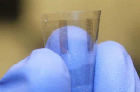
Printed semiconductor circuit printed on nano paper - (Photo: University of Maryland)
This is a paper made from enzymatic pulp and processed under mechanical action.
They create semiconductor circuits on the surface of nano paper by printing different types of ink, including a layer of carbon nanotubes, dielectric ink, semiconductor ink and another layer of nanotubes, according to the report. and Flexible Nanopaper Transistor.
Experts explain that the semiconductor circuit has unique characteristics, such as plasticity, reasonable cost, light weight and alternative energy use.
Currently 'green' electronics are becoming a potential field of research, increasingly receiving the attention of manufacturers.
Up to 84% of new semiconductor circuits are transparent, ductile, allowing it to remain active when lightly bent. Meanwhile, nano paper is thin enough to be cut or folded, paving the way for electronic generations to fold. According to Extreme Tech, lead researcher Liangbing Hu, nano-thin paper like plastic.
The next challenge researchers are aiming to find a way to print nano-paper at a mass production level for commercial purposes.
- Actual photo of Windows 10X on ThinkPad X1 Fold
- [CES 2020] Lenovo ThinkPad X1 Fold, the world's first folding laptop, costs $ 2,500
- Leaking images of new patents by Google: Challenges of the folding screen market in the future?
- Struggling the folding screen smartphone of the drug lord's brother: It's just the Galaxy Fold with more gold decals
- How does a folding phone work?
- Explore the inside of Galaxy Fold, impressive sorted components, flexible screen


 How to create A3 and A4 paper sizes in Photoshop
  Instructions on how to align beautiful margins for A4 paper size in Word
  How to print A5 size paper in Word
  Paper size in Photoshop
  How to fix Epson L805 printer error flashing 5 lights continuously