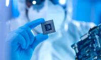
Close-up of the $ 150 million machine that dominates the global semiconductor industry
ASML's photolithography machine is the most important component of the world's leading semiconductor chip manufacturing process. Each machine costs 150 million USD.
Photolithography is the process of shining a light ray towards a silicon wafer (wafer) through a pre-drawn glass disc to print the circuit diagram onto the photosensitive surface of the silicon wafer. In order to print smaller circuits, lamps with shorter wavelengths are needed. Currently, the most current is ultra-ultraviolet (EUV).
ASML is a Dutch technology company. In 2017, the company launched the first EUV lithography machine.
Each EUV machine now has 100,000 parts and a total cable length of about 2 km. It's about the size of a bus and costs $150 million. It takes up to 40 containers, three transport planes and 20 trucks to transport components for an EUV machine.
There are only a few companies in the world that can afford to buy ASML's EUV machines, most of which belong to TSMC, Samsung and Intel - the three largest semiconductor chip manufacturers in the world.
Will Hunt, an analyst at Georgetown University in the US, said that it is impossible to make state-of-the-art chips without ASML's machine.
Manufacturing microprocessors requires the most modern techniques in the world. The semiconductor chip starts from a cylindrical silicon crystal, which is neatly cut into thin wafers and coated with a light-sensitive material. It is then exposed continuously to certain shaped rays of light. Using chemicals to remove parts that are not exposed to light to create electronic circuits. The wafers are then cut to create individual chips.
Electrons move more efficiently with smaller components. In addition, increasing the number of components on the chip will increase the overall computing power. So the best way to increase the processing power of each chip is to shrink the components.
Earlier deep ultraviolet (DUV) technology used light at 193 nanometers. Currently, EUV uses light with a wavelength of 13.5 nanometers.
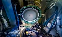
To create a strong light beam, ASML applies a method of shining a high-powered laser at a tiny tin droplet up to 50,000 times/second.
Ordinary lenses absorb EUV light, so to correct the direction of light rays, the machine must use mirrors coated with special materials with extremely high precision. The EUV rays inside the machine are reflected through many mirrors, then hit the glass dish containing the circuit diagram.
EUV arrives 20 years late and costs 10 times more than expected, but it is currently the only tool for making extremely close-knit architectures.
ASML's new machine adds a new method of making chips with a resolution of 13 nanometers. The company adds that the next generation can engrave details as small as 8 nanometers.
Was this article helpful?
Your feedback helps us improve.
Related Articles
 UK pours £1 billion in semiconductor industry funding3 minutes read
 Semiconductor industry revenue to increase 18% in 2024, Samsung regains number one position3 minutes read
 China 'pumped' nearly 2 billion USD of investment into the country's largest memory chip manufacturing company3 minutes read
 The US may place a series of limits on Korean semiconductor chips made in China4 minutes read
 Galaxy A51 dominates the segment with many outstanding features4 minutes read
 Glowing silicon: The key to big strides in the semiconductor industry2 minutes read
Reader Comments 0
Sign in with email or Google to join the discussion.