Learn about how the CPU works (Part II)
In the previous lesson, we learned the basic information about Clock and External Clock that works in the CPU, this article will continue with the diagram of a CPU and memory storage.
CPU (Central Processing Unit) - also called microprocessor or processor - is a central data processing unit. Although each processor has its own design, it all has the same general principle - this is exactly what we want to introduce to you in this article. We will introduce the most general CPU architecture so you can understand more about Intel and AMD products as well as the basic differences between them. In the previous lesson, we learned the basic information about Clock and External Clock that works in the CPU, this article will continue with the diagram of a CPU and memory storage.
- Learn about how the CPU works (Part I)
Block diagram of a CPU
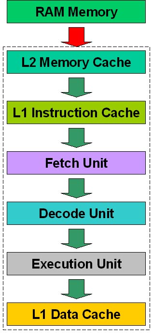
On Figure 6 you can see a basic block diagram of a modern CPU. There are many differences between AMD and Intel architectures. Understanding this basic knowledge will be a step for you to understand how Intel and AMD CPUs work and the differences between them.

Figure 6: Basic block diagram of a CPU
The dotted line on Figure 6 shows the 'body' part of the CPU, since the RAM is placed outside the CPU. Data datapath between RAM and CPU is usually 64-bit (or 128-bit when using dual-channel memory configuration), using memory clock or CPU external clock (low clock). The number of bits used and clock rate can be combined in a block called transfer rate, in MB / s. To calculate the transfer rate, the formula is calculated using this number of bits x clock / 8. With a system using DDR400 memory in a single channel configuration (64 bit), the transfer rate will be 3,200MB / s, and the same system using dual channel (128 bit) memory will have speed Memory transmission is 6,400 MB / s.
All circuits inside the dot markings run at the CPU clock rate. Depending on the CPU, some parts of it can run at higher clock speeds. Also, data paths between CPU blocks can be wider, meaning more bits are transmitted per clock cycle 64 or 128. For example, data lines between L2 cache and L1 instruction cache on sets Modern processors are usually 256 bits. The higher the number of bits transmitted per clock cycle, the faster the transmission will be performed (in other words, the higher the transmission rate). In Figure 5, we used a red arrow between RAM and memory cache L2; arrows between other blocks to describe the different clock speeds and widths of the data lines used.
Memory Cache
Memory Cache is a type of high-performance memory, also called static memory. The type of memory used on the computer's main RAM is called dynamic memory. Static memory consumes more power, is more expensive and has a larger physical size than dynamic memory, but it runs faster. It can work with the same CPU clock rate, which dynamic memory cannot perform.
Entering the 'outside world' to fetch data causes the CPU to work at a lower clock rate so that the memory cache technique is used here to overcome this drawback. When the CPU loads data from a certain memory location, the circuit called the memory cache controller (this circuit is not drawn in Figure 6) loads into the memory cache a data block below the current position that the CPU has loaded. Because the programs are executed in order, the next memory location that the CPU will require can be the location just below the memory location it has loaded. Because the memory cache controller has loaded a lot of data under the first memory read by the CPU, the next data will be inside the memory cache, so the CPU does not need to perform external data manipulation: it has been loaded inside the memory cache embedded in the CPU, precisely because it is embedded in the CPU that they can access with the internal clock rate.
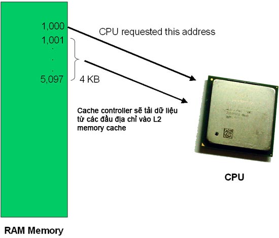
The cache controller always observes the memory locations that are being loaded from some memory location after the memory location has been read. A real example, if a CPU loaded data is stored at address 1,000, the cache controller will load data from the 'n' address after the 1,000 address. The number 'n' is called a page; If a microprocessor works with 4KB page (typical value), it will load data from 4,096 addresses under the current memory location being loaded (1,000 address in the example). 1KB equals 1,024 bytes, so 4,096, not 4,000. We have shown this example in Figure 7.

Figure 7: How memory cache controller works
The larger the memory cache, the higher the chances for data required by the CPU here, so the CPU will reduce direct access to RAM, thus increasing system performance (when the CPU needs direct access. In RAM, it must perform at a lower clock rate, thus reducing the overall system performance.
We call 'hit' when the CPU loads a request data from the cache and 'misses' if the requested data is not there and the CPU needs to access the system's RAM.
L1 and L2 are 'Level 1' and 'Level 2' respectively, representing the distance from them to the CPU core (execution block). A good doubt is why there are up to 3 cache (L1 data cache, L1 instruction cache and L2 cache). Notice in Figure 6 that you will see that the L1 instruction cache works as an 'input cache', while the L1 data cache works as an 'output cache'. The L1 instruction cache - usually smaller than L2 cache - is only effective when the program starts to repeat a small part of it (loop), because the required instructions will be closer to the fetch block.
On the technical details page of a CPU, L1 cache can be represented by a completely different image. Some manufacturers list two separate cache L1 (sometimes call the instruction cache 'I' and the data cache is 'D'), some firms write the number of both as 128 KB but that means is 64 KB for instruction cache and 64 KB for data cache. However, for later Pentium 4 and Celeronn CPUs based on socket 478 and 775 there is no such phenomenon.
Pentium 4 processors (and socket 478 and 775 Celeron processors) do not have an L1 instruction cache but instead have a trace execution cache, this is the cache placed between the decoding block and the real block exam. So this is the L1 instruction cache but the name has been changed and in a different location. We are talking about this because this is a very common mistake when thinking that Pentium 4 processors do not have L1 instruction cache. So when comparing Pentium 4 with other CPUs, think that its L1 cache is much smaller.
Branching
But we have mentioned a few times before, one of the main problems for CPUs is that there are too many "miss" for the cache, because the fetch block must access RAM directly (slow ), should slow down the whole system.
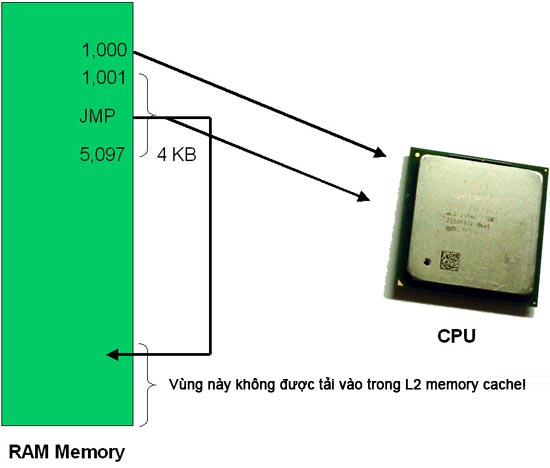
Often using a memory cache avoids many of these problems, but a typical solution to this problem is branching: If in the middle of the program there is a JMP ('jump' or 'go to' command) ) sending the program to a completely different memory location, this new location will not be loaded in the L2 memory cache, but will only make the block fetch that location directly in the RAM memory. To solve this problem, the cache controller of the modern CPU analyzes the memory block it has loaded and whenever a JMP instruction is found it will load the memory block into that location in the previous L2 memory cache. when the CPU processes that JMP instruction.

Figure 8: Unconditional branch solution
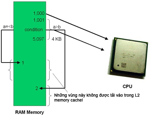
This results in much easier implementation, the problem is that when the program has a conditional branch, that is, the address that the program will enter depends on a condition that is not yet known. For example, if a = b then enters address 2. We illustrate this example in Figure 9. This will create a 'miss' for the cache, because of the The values of a and b are completely unknown and the cache controller will only be looking at JMP-like instructions. The solution here is: the cache controller loads both conditions into the memory cache. After the CPU processes the branch instruction, it will simply remove an unchecked case. Loading the cache with unnecessary data is better than accessing the RAM memory.

Figure 9: Conditional branch solution
- Learn about how the CPU works (End)
- Learn how Cache works (Part 2)
- How Phishing works
- Learn about how email works
- Learn how cache works
- Network basics: Part 2: Understanding the Router
- Learn about WebMatrix - part 2
- How the botnet works (Part 2)
- How Hacker works
- What is the Wininit.exe program and why it always works
- Learn about the SearchIndexer.exe process and why it works


 How to increase browser buffer size for better performance
  How to clear cache in Google Drive and Docs
  How to clear the Cache in Windows 8?
  How does CPU Cache work? What is L1, L2 and L3 Cache?
  How to delete cache and cookies on Chrome, Firefox and Coc Coc
  How to optimize Delivery Optimization cache in Windows 10