Learn about FlipChip technology
If you are not sure about the term 'FlipChip', this guide will help you better understand the FlipChip packaging technology (also known as flip-chip packaging)..
If you are not sure about the term 'FlipChip', this guide will help you better understand the FlipChip packaging technology (also known as flip-chip packaging).
The FlipChip package technology has existed for three to four decades, with the original role as a solution for the large number of batteries (pins) and high performance requirements. At first, the majority of the FlipChip package applications were SoC with a large number of batteries (including more than 700 batteries), which the Wire-Bond BGA package typically cannot handle properly. In addition, some SoCs incorporate high-speed interfaces (including RF) that wirebonds (the process of connecting wires on chip bases with extremely thin fibers from chip circuits) may not support Support due to high resistance of the wire.
The demand for the FlipChip package has increased over the past decade and is driven by the mobile market, where packet size and signal performance play a very important role.
Today, the FlipChip package technology offers a range of benefits including: Large battery numbers, high signal density, better dispersion capacity, low signal resistance and good ground / power connections. The FlipChip package is quite popular today and you can find them in small devices like high-end mobile phones.
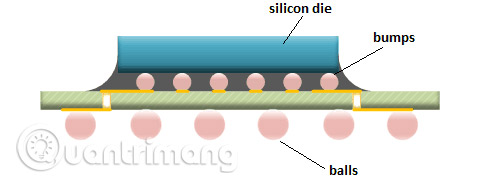
Basically, the name FlipChip describes the method used to connect a semiconductor mold to a chip base. In a FlipChip package, the molds are bumped and then flipped onto the chip base, so it's called FlipChip.
Due to the fact that bumps (yellow balls) are distributed over the entire chip, not just on the edge of the mold, so the pad (pads) can be placed across the mold surface. This allows designers to place more pad for each mold, reduce chip size and optimize signal integrity.
The chip base provides the ability to connect to the external PCB through solder ball (lead ball). Chip size, number of layers and material properties have a direct impact on the total cost. In some cases, the chip base may be the most expensive element in the FlipChip package.
The bumps are placed directly on the I / O pad and therefore, they connect the mold to the base. After the bumping process (bumping is an advanced wafer processing technology, in which, solder ball / bump is formed on the wafers), the wafer is broken down and finally, the mold will flip onto the base chip. The bumps connect mold and chip base together into a single package.
Chip base technology
The FlipChip chip is a small PCB inside the package and very similar to any other PCB. The difference is that the chip base size is much smaller than most PCBs you have seen.
Design the chip base to include the layout of all signals from the outer package to the bump pad.
Chip base can be made of many different materials: Laminate, porcelain, etc. Wood chip design rules of vendors are not the same.
The chip base may consist of several layers, ranging from 2-18 layers to allow routing of all signals.
Wafer Bumping Technology
The bump wafer provides a connection between the mold and the chip base, through low resistance and resistance, as well as reliable, high quality production materials.
The bump wafer can be made of high-quality, lead-free, lead-free, high-lead or Cu pillar technology. The size and bump distance of each assembler is not the same.
FlipChip assembly process
In the final wafer processing step, the bumps placed on the chip's pad can be found on the top of the wafer. In order for the chip to be connected or attached to the base, the mold is flipped and aligned with the pad on the base.
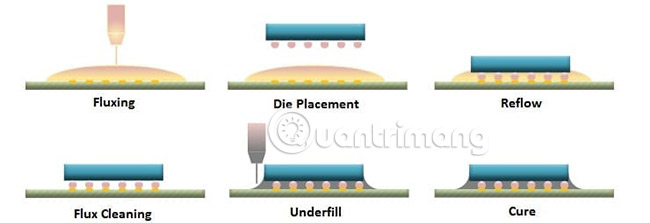
There are 6 steps in the FlipChip creation process, which gives it considerable flexibility when connecting devices.
Pros and cons of FlipChip
FlipChip packages have advantages and disadvantages, derived from assembly methods that create a much more compact chip than previous wirebond solutions. Because the chip is directly connected to the circuit board, the wire is shorter, resulting in less resistance. This means that the devices can now transmit signals at significantly higher speeds and at the same time dissipate heat more efficiently.