Table of Contents
This guide covers inside pentium m architecture with practical context and easy-to-follow details. Use it to understand the subject and apply the information confidently.
Gabriel Torres
On the outside, Pentium M works like Pentium 4, transmitting 4 data per clock cycle. This technique is called QDR (Quad Data Rate) and makes the internal bus more than quadruple in performance with its actual clock rate, you can see the table below.
Real ClockPerformanceTransferRate
100 MHz
400 MHz
3. 2 GB / s
133 MHz
533 MHz
4. 2 GB / s
-
L1 memory cache: Two L1 memory cache 32 KB, one for data and one for instruction (Pentium III has two L1 memory cache16 KB).
-
L2 memory cache: 1 MB on 130 nm models ('Banias' core) or 2 MB on 90 nm models ('Dothan' core). Pentium II only has 512 KB. Celeron M, Pentium M's cheapest version also has 512 KB of L2 memory cache. Support for SSE2 instructions.
-
Advanced branch prediction: Branch prediction has been redesigned (and based on Pentium 4's circuit) to improve performance.
-
Consolidation of many small operations: The instruction decoder unites two small actions into one to save energy and improve performance. We will talk more about this in the next section.
-
Advanced SpeedStep technology, this technology allows CPUs to reduce the clock in idle mode to save battery life. A number of battery-saving features have also been added to Pentium M's microarchitecture, for the purpose of these CPUs was originally designed for mobile computers.
Now let's take a closer look at Pentium M. Architecture. Pentium M's principle The principle is a list of all layers that the given instruction must be executed in accordance with the algorithm. Intel did not disclose Pentium M's principles, so we will talk about Pentium III's principle. Pentium M's principle is likely to have more levels than Pentium III but analyzing it will give us an idea of how Pentium M architecture works. Remember, the Pentium 4 working principle has 20 floors and the working principle of newer Pentium 4 CPUs is based on 'Prescott' core with up to 31 floors. On Figure 1 you can see the Pentium III 11-storey principle
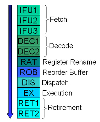 Figure 1: Pentium III Principle
Below we will explain basically about each layer, explaining how each assigned instruction is done by the P6 class processors. This will not be as complicated as you think. This is only a summary and the specific explanations will be given below.
-
IFU1: Load a line (32 bytes equivalent to 256 bits) from the L1 cache instruction and store it in the instruction flow buffer (Instruction Streaming Buffer).
-
IFU2: Identify boundary instructions (16 bytes equivalent to 128 bits). Since x86 instructions do not have a fixed length, this layer marks the location where each instruction starts and ends within the loaded 16 bytes. If there is any branch within 16 bytes, the address it has will be stored at the Branch Target Buffer (BTB), so the CPU can use this information later on to strongly predict its branch.
-
IFU3: Mark the instruction decoder unit of each instruction to be sent. There are three different instruction decoding blocks that we will cover in the next section.
-
DEC1: Decode the x86 instruction into small RISC instructions (small operations). Since the CPU has up to 3 instruction decoders, it can decode up to 3 instructions at the same time.
-
DEC2: Sending small decoded instructions to the decoded Instruction queue (Decoded Instruction Queue), this queue can store up to 6 small instructions. If the instruction has been converted more than 6 small instructions, this layer needs to be repeated in order not to miss them.
-
RAT: Because the P6 architecture performs out-of-order execution (not in order, abbreviated to OOO), the value of the given register can be changed by a previously executed instruction Program location takes place, corrects necessary data for other instructions. Therefore, to solve this type of conflict, at this level, the original register used by the instruction will be changed to 40 internal registers that the micro architecture that P6 has.
-
ROB: At this stage, three small instructions decrypted will load into the Reorder Buffer (ROB). If all data is needed for the execution of a small instruction provided and if there is an open slot in the Reservation Station decrypted queue, this instruction will be moved to this queue.
-
DIS: If this decrypted instruction is not sent to the above queue, it can be done at this level. The decoding instruction will be sent to the appropriate execution block.
-
EX: The decoded instruction will be executed at this execution block. Each of these decoded instructions needs only one clock cycle to be executed.
-
RET1: Check in the Reorder Buffer buffer to see if any decoded instructions are marked as 'executed'.
-
RET2: When all decoded instructions are related to the x86 instruction that has actually been removed from the Reorder Buffer buffer and all the small (decoded) instructions are associated with the current x86 instruction The operation has been executed, these instructions will be removed from the Reorder Buffer buffer and x86 registers will be upgraded (the process is returned to the RAT layer). The process of returning to work must be done in order. The three decoded instructions can be removed from the Reorder Buffer buffer per clock cycle.
Below we will introduce more detailed information for you to understand its operation. Memory Cache and Fetch Block But we mentioned earlier, Pentium M's L2 memory cache could be 1 MB on 130 nm models ('Banias' core) or 2 MB on 90 nm models ('Dothan' core). Meanwhile it has two L1 cache memories, one is 32KB for instructions and the other is 32KB for data. As explained in the previous section, the fetch block is divided into 3 layers. In Figure 2, you can see how the fetch block works.
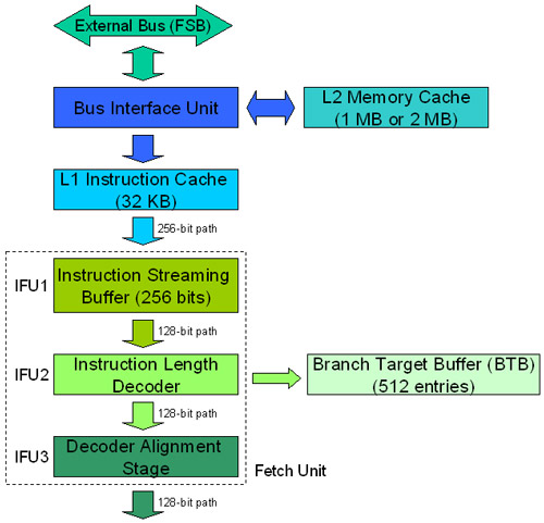 Figure 2: Fetch block
The block fetches the first row (32 bytes = 256 bits) into its instruction flow buffer (Instruction Streaming Buffer). Then the instruction-length decoder will recognize the instructional boundaries inside every 16 bytes. Since the x86 instruction does not have a fixed length, this layer marks the location where each instruction starts and ends within the loaded 128bit. If there is a branch instruction within those 128 bits, the address is saved to the Branch Target Buffer (BTB), so your CPU can use this information later on its branch prediction. BTB has 512 inputs. After the Decoder Alignment Stage layer marks which instruction decoder block each instruction will be sent. There are 3 different instruction decoding blocks that we will cover below. Solve the instruction code and change the name for the register Because the P6 architecture is used for hybrid Pentium Pro processors with hybrid CISC / RISC, the processor must accept CISC instructions and is also known as x86 instructions, this is due to All software provided today is written in this type of instruction. CPUs using only RISC are not created for computers, because they do not run current software such as Windows and Office. Therefore, the solution used by all processors currently offered on the market today from both Intel and AMD is to use CISC / RISC decoding. Inside, the CPU processes RISC instructions but its front-end only accepts CISC x86 instructions. CISC x86 instructions are referred to as regular instructions and internal RISC instructions are referred to as decoded instructions. However, RISC decoded instructions cannot be accessed directly, so we cannot create software based on these instructions to bypass the decoder. Also, each CPU uses its own RISC instructions, these instructions are not published and are incompatible with decoded instructions from other CPUs. That means that Pentium M's decoded instructions are completely different from Pentium 4's decoded instructions, the difference is from Athlon 64 decoding instructions. Depending on the complexity of the x86 instruction, it must be converted into RISC decoding instructions. Pentium M instruction decoder works the same as shown in Figure 3. As you can see, there are three decoders and a decoded instruction sequencer (MIS). Two decoders are optimized for simple instructions, in which simple instructions are often just a decoding instruction. This type of instruction is converted as a decoding instruction. A decoder optimized for complex x86 instructions, this instruction can be converted into 4 decoded instructions. If the x86 instruction is too complex, meaning it converts to more than four decoding instructions, it will be sent to MIS as ROM memory, including a list of instructions that can be used to replace x86. On.
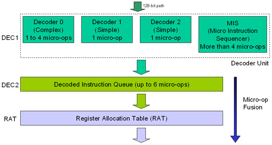 Figure 3: Decoder and rename register
The instruction decoder can convert up to 3 x86 instructions per clock cycle, a complex decoder 0 decoder 0 and two simple decoders 1 and 2, which makes us feel Decoded Instruction Queue can be up to 6 decoding instructions per clock cycle, possible scenario when Decoder 0 sends 4 decoded instructions and two other decoders send each a set of instructions has been decoded - or when the MIS is used. Complex x86 instructions used (MIS) The Micro Instruction Sequencer can slow down a number of clock cycles when decoding, depending on the number of decoded instructions generated from the conversion. You should note that the Decoded Instruction Queue can only hold up to 6 decoded instructions, so if there are more than 6 decoding instructions generated by the decoder plus MIS then another cycle will be used to send the current instructions in the queue to the Register Allocation Table (RAT), empty the queue and accept the decoded instructions that did not match it before. Pentium M uses a new concept for P6 architecture, this concept is called decoding instruction integration. On Pentium M, each decoder connects two instructions that have been decoded into one. They will only be separated when executed, at the execution layer. On P6 architecture, each instruction is 118 bits long. Pentium M instead of working with 118bit instructions, it works with instructions that are 236bit long, which is the join size of two 118bit instructions. You need to be aware that the decoded instructions are 118bit long, and what is changed is that they are conveyed into a group of two basic instructions. The idea behind this method is to save energy and increase performance. Sending an instruction that is 236bit long is faster than sending two 118bit instructions. In addition, the CPU will consume less power because there will be fewer decoded instructions circulating inside it. The instructions attached will then be sent to the Register Allocation Table (RAT) table. CISC x86 architecture has only 8 32-bit registers that are EAX, EBX, ECX, EDX, EBP, ESI, EDI and ESP. This number is too low because modern CPUs can execute out-of-order code, and it will "ruin" the content inside the existing register, thereby causing programs to fail. Therefore, at this stage, the processor changes the names and contents of the registers used by the program to one of the 40 internal registers already available (each of which has 80 bits wide, thus accepting both raw data and changing data), allowing the instruction to run at the same time with other instructions that use the same standard register, or even out-of-order This means that the second instruction can run before the first instruction even if they are on the same register. Reorder Buffer buffer When x86 instructions and decoded instructions have transmission results that keep the CPU layers in the same order, they appears on the running program. When entering the ROB, the decoded instructions can be loaded and executed out-of-order by the execution units. After executing, the instructions are sent back to the Reorder Buffer. Then at the Retirement, the executed instructions are output from the Reorder Buffer buffer with the same order they were loaded, meaning they are transferred in order. On Figure 4, you can get an idea of how they work.
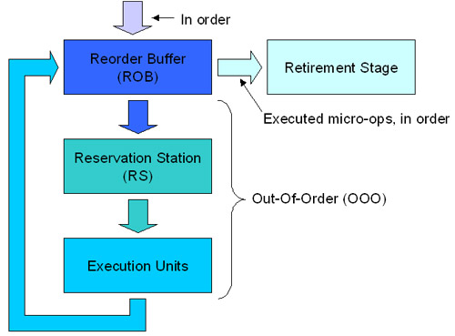 Figure 4: How the Reorder buffer works
In Figure 4, we have simplified the Reservation Station and execution units to make it easier to understand this buffer. We will talk about these two layers further in the lower part. Reservation Station and execution blocks As we mentioned earlier, Pentium M uses linked instructions (usually two instructions are connected) from the decoding block to the location of the sent ports located on the Reservation Station. Reservation Station sends decoding instructions separately (split paired). Pentium M has 5 such ports, these ports are numbered from 0 to 4 on Reservation Station. Each port is connected to one or more execution blocks, as you can see in Figure 5.
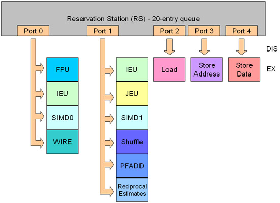 Figure 5: Reservation Station and execution blocks
Here is a brief explanation of each implementation block on this CPU:
-
IEU: Instruction Execution Unit - The instruction execution block is where instructions are usually executed. Also known in the introductory books on computer structure with the name ALU (Arithmetic and Logic Unit). These common instructions are also referred to as 'integer' instructions.
-
FPU: Floating Point Unit is where complex mathematical instructions are executed. Previously, this block was also called 'math co-processor' - a co-processor of math.
-
SIMD: where SIMD instructions are executed, ie MMX, SSE and SSE2.
-
WIRE: Complex functions
-
JEU: Jump Execution Unit processes branches and is also known as Branch Unit.
-
Shuffle: This block executes a type of SSE instruction called 'shuffle'.
-
PFADD: Execute an SSE instruction called PFADD (Packed FP Add) and both COMPARE, SUBTRACT, MIN / MAX and CONVERT instructions. This block is provided separately, so it can start executing a new decoding instruction every clock cycle even if it does not complete the execution of the decrypted instruction first. This block has a clock delay of three cycles, meaning that it will keep the clock cycle slow for each instruction that has been processed.
-
Reciprocal Estimates: Execute two SSE instructions, one is called RCP (Reciprocal. Estimate) and another is called RSQRT (Reciprocal Square Root Estimate).
-
Load: This block is used to process commands that ask data to be read from RAM.
-
Store Address: The block that handles instructions asking data to be written in RAM. This block is also called AGU, Address Generator Unit. This type of instruction uses both Store Address and Store Data blocks at the same time.
-
Store Data: Handle instructions that ask data to write to RAM memory. This type of instruction uses both Store Address and Store Data blocks at the same time.
VoltageClock 1. 484 V1. 6 GHz1. 42 V1. 4 GHz1. 276 V1. 2 GHz1. 164 V1 GHz1. 036 V800 MHz0. 956 V600 MHz
Each Pentium M model has its own voltage / clock table. One thing to keep in mind is that when you don't need a lot of power for a laptop, it not only reduces the clock rate but also reduces the voltage, reducing the voltage will reduce the consumption of many batteries. Enhanced SpeedStep technology works by checking specific model registers MSR (Model Specific Registers) of the CPU, which is called Performance Counter. With the information obtained from this department, the CPU can reduce or increase its clock / voltage depending on the usability of the CPU. Simply if you increase the CPU usage, it will increase the clock / voltage and if you reduce the CPU usage, it will reduce the clock / voltage. Enhanced SpeedStep is just one of the enhancements made with Pentium M microarchitecture that aims to increase battery life.
FAQ
What should I check before following these steps?
Confirm device and software compatibility, save important data, and make sure you have the required permissions, files, and account access.
Why might the process not work?
Common causes include outdated software, missing permissions, incompatible hardware, an unstable connection, or completing a step in the wrong order.
Can I undo the changes if necessary?
That depends on the tool or setting. Use built-in restore options when available, keep a backup, and record the original configuration first.
Related Articles
 Intel Pentium CPU Explained11 minutes read
 What Is Intel Pentium Chip? Performance of Intel Pentium CPU11 minutes read
 Pentium 4 CPU Upgraded to Windows 113 minutes read
 Test About Computer Architecture P64 minutes read
 Test of Computer Architecture P54 minutes read
 Intel 300: Complete Guide4 minutes read
Reader Comments 0
Sign in with email or Google to join the discussion.