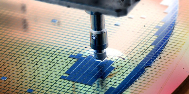
Samsung plans to mass-produce 5nm chipsets in Q2 2020
Samsung is still trying to upgrade the technology to gain more market share for processing chips from TSMC.
As the world's second largest chipmaker after TSMC, Samsung has begun mass-producing chipsets on its 6nm and 7nm EUV (Extreme UltraViolet) technologies. However, not wanting to stop here, the company has now announced plans to mass-produce 5nm chipsets from Q2 2020.
In addition, the company says it will continue to invest in more advanced processes as well as the 3nm GAA process. The Samsung V1 factory in Hwaseong, South Korea, will be in charge of this production. This is a special factory equipped with the most modern technology available today and capable of producing 3nm chipsets.

There have been rumors recently about a partnership between Google and Samsung to create a new processor for Google's Pixel phones coming next year. This 5nm chipset is expected to feature an 8-core CPU set with 2 Cortex-A78 cores, two Cortex-A76 cores and four Cortex-A55 cores. The chipset is expected to be Mali MP20 based on Borr microarchitecture. In addition, rumors also suggest that this chipset will be equipped with both Google's Visual Core ISP and NPU, instead of using Samsung technology.
If these rumors are accurate, this could be seen as a new step for Samsung's semiconductor outsourcing division in the race with TSMC. A few months ago, it was rumored that the department had won a contract to process a new 5G modem for Qualcomm.
In order to gain more customers from its business rival, Samsung is expected to start mass production of 3nm chipsets by 2021, but it seems that the effects of the Covid-19 pandemic have forced the company to postpone work. Chipset production on new process until 2022.

Reports suggest that the pandemic has hindered the ability to find orders to fill the schedule for Samsung's new process production line. The Korean company's 3nm process is based on GAAFET (Gate All Around) technology, instead of FinFET like other competitors. Samsung's technology is said to be able to reduce transistor size by 35% while providing 50% higher energy efficiency.
The difference in GAAFET's design is that the gate is located around all 4 sides of the channel, instead of just placed on both sides as the FinFET design. This design helps to ensure a significant reduction of leakage current through the channel and better control of the current flowing through that channel.
Discover more
mass production samsung factory processor transistor chip productionShare by
Isabella HumphreyYou should read it
- Samsung, Xiaomi, Oppo and LG all simultaneously closed production plants in India
- China's memory chip production will go from zero to 5% of the world by the end of next year
- Samsung began mass-producing the world's 'fastest memory' for smartphones
- 6 ways to apply AI in music production
- Close-up of how the medical mask production line operates?
- The Quiet Details That Make a Sports Betting Platform Feel Reliable
- Instructions on creating toy set images with ChatGPT AI
- How are AI agents changing the journalism industry?
- What is a NAS hard drive? What is a Surveillance Hard Drive?
- PUBG adds bots to 'support' new players or approaching death
- How to display the File Pane Preview Pane on Windows 10