Why Miniaturization Remains the Biggest Challenge for Advancing Technology in Wearables
Wearable devices are now truly amazing, but they're not as exciting as most people see them. It's not difficult to make a breakthrough in step counting, blood oxygen monitoring, and notification execution..
The difficult part is that everything needed to run those functions is installed in something that can be worn on the wrist or attached to the ear without overheating, consuming six hours of power, or being large and heavy. Like a hockey puck.
The first major breakthrough in this area will not be achieved through smarter algorithms, but through the use of better materials and more rigorous engineering at very small scales.
The power-to-size paradox has no easy solution
The pace of battery innovation is slow compared to the advancements in processing. This is the gap that wearable designers must face every day. Users demand a device that can last two days on a single charge, constantly monitor their heart rate, use GPS, and still be discreet under their shirt. These expectations are contradictory.
Energy density, which is the amount of charge a cell can store for its physical size, is the main bottleneck. The reduction of a battery does not simply reduce the capacity in a linear way; it also changes the discharge, thermal, and mechanical characteristics. Designers cannot just scale down a big battery and expect the performance curve to be the same. They need to re-design everything to adapt to what a smaller cell can provide. And this would be the processor, the sensors, and the communication radios that also need to get more power efficient in parallel.
The wearable technology market is expected to grow with a compound annual growth rate of 14.6% from 2023 to 2030 (Grand View Research), with the health monitoring features that require ever-increasingly dense internal hardware to be a leading driver. This growth represents real pressure on an engineering problem that does not have a comfortable solution yet.
Heat has nowhere to go
A desktop computer can be equipped with fans, vents, and heat spreaders. In contrast, a wearable is built with a sealed enclosure, often in direct contact with the skin, and without any active cooling mechanisms. For example, when you tightly integrate a SoC, multiple bio-sensors, wireless radios, and power management circuits within a space that's even smaller than a matchbook, the heat produced by all of those parts must be pushed through the device's casing and into the ambient air - or the user's skin.
Thermal management within miniaturized devices becomes a situation whereby you must purposefully worry less about moving heat away from individual parts and instead concentrate your efforts on doing everything you can to keep it from building up in the first place. This can result in lower-power design choices that negatively impact performance or even necessitate the use of different materials with superior passive thermal properties. Neat and tidy tradeoffs aren't guaranteed.
There's also the issue of the long-term durability of components when subject to excessive heat over periods of time. A device that continuously runs warmer will also ultimately fail far sooner than a product with parts that function within their rated tolerances. In products that consumers may reasonably expect to be using at least a few years for example, the two- to three-year life of many consumer products today indeed is a very real concern.
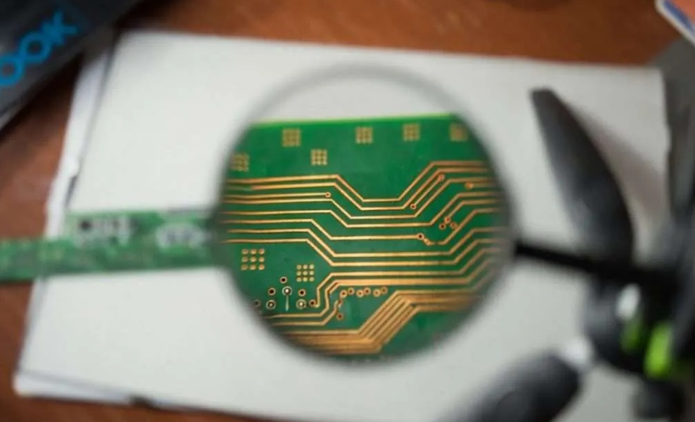
Why circuit board architecture is where material science matters most
High-Density Interconnect PCBs - HDI boards - are the structural backbone of modern wearables. They allow more circuitry to be packed into less surface area through tighter trace routing and multiple stacked layers. But squeezing layers together creates its own set of problems around signal integrity and electromagnetic interference.
When signal traces run close to each other at high frequencies, they can corrupt each other's data. EMI shielding and careful layer arrangement reduce this risk, but material quality becomes equally important. A conductive layer that's slightly impure or inconsistent in thickness will cause signal losses and interference that testing won't always catch until the device is in the field.
This is where the choice of PCB copper foil material directly affects electrical performance. As foil layers get thinner to reduce overall board thickness, conductivity can't be traded away to get there. The foil has to maintain consistent grain structure and surface smoothness at reduced thickness - properties that require tighter manufacturing controls than standard PCB production demands.
The human factor cuts both ways
Proper ergonomic design is essential for wearables. The closer a bio-sensor can be to the skin, the better and more accurate the information it returns will be. Material selection and device form factor determine how comfortably a wearable can be worn for long periods of time. Size decisions often seem fragmented: aesthetic, electrical, mechanical, thermal, and power design engineering trade-offs compete and often lack a feedback loop from the human wearer. Smaller and thinner, for example, seem like clear goals, until the device has to be worn by a real human.
The honest picture of wearable development is a chain of physical constraints, each one affecting the next. Better materials allow thinner boards. Thinner boards enable smaller form factors. Smaller form factors demand more efficient power and thermal design. Software makes the device useful, but the materials make it possible.