Why is the CPU or rectangular camera sensor created from a circular plate?
Why didn't people create rectangular wafers or squares in the first place to cut out CPU and image sensors without wasting?
For computers and cameras, CPU and image sensors are two extremely important components such as the 'brain' of the device. With computers, CPUs act as processing centers, have the ability to calculate and control the operation of all other components.
With cameras, image sensors are components that play a decisive role in the existence of digital photography industry. The image sensor is responsible for capturing light, turning it into a digital signal that can be stored into images.

A wafer is used to make computer CPUs.
Semiconductor sensors made in large quantities on a circular silicone sheet are called 'wafer' and not made separately. From a wafer it is cut into sensors and cutting rectangular pieces from a circular object will lead to problems with excess material.
In fact, a wafer can produce 244 1-inch sensors with an excess area of 12.6%; APS-C sensor (crop x1.5) with 18% redundancy; 20 - 24 camera sensors in Full-frame format and 36% excess area. No matter how small people try to cut, there is still an area left.

Image sensor is cut from a wafer.
These wafers are quite expensive. It is estimated that a high quality 8 inch diameter silicone sheet can cost up to 5000 USD. So why didn't people create rectangular wafers or squares in the first place so that when cutting out CPUs and image sensors were not wasted?

A big silicone ingot.
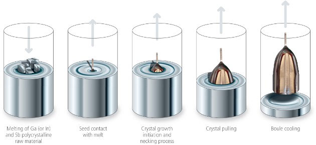
The reason the wafers are made round is because of the way people create it. The first shape of a semiconductor wafer is a very large cylindrical 'lump' called a silicone ingot, made with the Czochralski process. This process was invented by Jan Czochralski, a Polish scientist.
Accordingly, pure silicone will be melted into liquid with a ratio of 1 / 10,000,000 non-pure atoms, very high purity. A silicone crystal stick is immersed in this liquid, then it has just been turned and pulled up slowly. The lower the temperature, the lower the silicone will cling to the core, and evenly distribute into a ingot thanks to centrifugal force.
Czochralski process.
The video explains the process of Czochralski.
When this ingot has cooled, people will use diamond cutting blades to cut them into small pieces with high accuracy. The sheets will be washed and polished to form a silicone wafer.
To save costs in this process, scientists only have the only method of gradually increasing the diameter of the silicone ingot. This means that the diameter of the wafer also increases, which in turn can make more products in a turn to increase productivity.
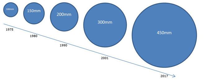
The size of the wafer gradually increases over time.
However, due to complicated manufacturing process and many standards need to be ensured, the cost of creating this product is still very high and the efficiency has increased. That is the reason only very few manufacturers of high quality camera and CPU sensors in the world.
- Samsung launches revolutionary 200MP camera sensor
- Megapixel or sensor size is more important for smartphone cameras?
- The formula for calculating rectangular box area, rectangular box volume
- Why is the camera sensor size on a smartphone more important than the number of 'dots'?
- iPhone 2019 will have a 3D sensor on the rear camera
- Not giving up the camera race, Nokia 9.3 PureView 5G will have 5 cameras, 108MP sensor?
- Samsung plans to launch smartphone with 600MP camera?
- Is the sensor vibration reduction technology unique, making Apple want to equip its new iPhone?
- How to check the original purchase date of the iPhone / iPad on Apple's website
- What is Google Camera Mod? What devices are supported and where are they downloaded?
- 12 am is AM or PM in English?
- Bad guys can steal data by freezing RAM sticks with liquid nitrogen
- Why does Winrar give you a free trial for a lifetime?
- Office 365 will have the new Unverified Sender feature
- There is an official version of Microsoft Office 2019 available, please download
- What's the Russian super officer's cell phone security that is twice as high as the iPhone X?
- WSL2 now supports connecting Localhost from Windows 10 applications
- 'Hack' the dinosaur game of Google Chrome to make your T-Rex immortal and max speed


 How to Coat Something in Silicone